Clock Generator User's Guide (TN-007): Difference between revisions
(Initial addition) |
m (→Block Diagram: Added picture of board) |
||
| Line 12: | Line 12: | ||
<center> | <center> | ||
[[Image:clockgen_blkdiag.png|650px]] | [[Image:clockgen_blkdiag.png|650px]] | ||
'''Clock Generator Block Diagram''' | |||
</center> | |||
<center> | |||
[[Image:clockgen_top.jpg|650px]] | |||
'''Clock Generator Block Diagram''' | '''Clock Generator Block Diagram''' | ||
Revision as of 23:59, 20 August 2008
This article describes the Clock Generator Module developed at the CSU-CHILL facility. It is capable of generating up to eight low-jitter clocks up to 1.6 GHz, depending on the configuration. Various logic families are supported, including LVPECL, LVDS and 3.3V CMOS. This design is primarily for the Solid-state X-band project, however, it is flexible enough to serve the needs of the CSU-CHILL and CSU-Pawnee radar systems.
Block Diagram
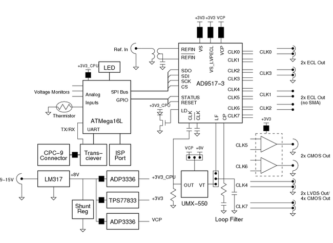
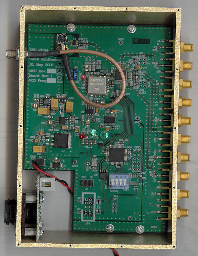
The figure shows a block diagram of the clock generator. An Atmel ATmega16L microcontroller is the primary control device. An Analog Devices AD9517 Clock Generator chip is used to implement the clock generation and distribution functions. The AD9517 is controlled by the ATmega16L through an SPI-compatible serial bus. In addition, the microcontroller monitors the AD9517's status through several general-purpose I/O lines. The AD9517 phase-locks a United Microwave UMX-550 1.92 GHz PLL to the input reference clock. The AD9517 outputs are brought out to ten SMA connectors.
The microcontroller communicates with a host machine through an RS-485 interface. The microcontroller firmware presents a Modbus/RTU interface, permitting external devices to program registers on the clock generator, and to poll its running status.
A significant portion of the design is dedicated to power supplies. This is to ensure that the clock generator chip and VCO are powered from clean, noise-free supplies to ensure the least possible jitter due to power supply ripple and noise.
The entire design is contained within an RF-tight aluminum enclosure to prevent leakage of the clock signals, and also to protect the VCO from external interference.
Clock Generator Block Diagram
Clock Generator Block Diagram
Components
Microcontroller
The microcontroller used on this design is the Atmel ATmega16L, a low-power 8-bit microcontroller with 16kB of Flash, 1k SRAM and 512 bytes of EEPROM. The ATmega series of controllers is chosen since they provide an inexpensive means of controlling remote devices, and open-source programming tools such as WinAVR are available. Several on-board peripherals are available, including an eight-channel ADC, timers, USART and general-purpose I/O. The microcontroller is clocked by a 7.3728 MHz crystal oscillator. The frequency is chosen to be a multiple of popular serial port baud rates such as 9600 bps.
The SPI port on the microcontroller is used to communicate with the AD9517 clock generator. This allows the MCU to set and read the registers on the AD9517.
The USART is used to communicate with a host through the Modbus/RTU protocol. A MAX3072 transceiver is used to perform level conversion and differential to single-ended conversion of the RS-485 bus. The MAX3072 controls the rise-time of the RS-485 bus to reduce the chance of interference.
The onboard 8-channel, 10-bit ADC is used to sample the various voltages present on the board, as well as to measure the board temperature using an NTC thermistor. The MCU performs linearization of the thermistor voltage, converting it to a temperature reading.
Reference Input
The reference frequency to which the PLL within the clock generator locks to is brought in through the reference input. An SMA single-ended input is used, and a Mini-circuits BALUN is used to convert this to a balanced signal. The balanced signal is fed to the Clock Generator chip. Proper biasing of the signals is necessary for the BALUN to function correctly.
The default configuration of the clock generator board accepts a 10 MHz reference frequency, at 0 - +10 dBm. By reprogramming the reference divider within the AD9517, any reference frequency up to 250 MHz may be used.
Clock Generator
The AD9517 clock generator performs the majority of the functions on the board. It consists of a 2.4 GHz PLL, an integral 2 GHz VCO and a clock distribution network. The clock distribution section of the chip includes various dividers that may be applied to the VCO output. Up to twelve outputs are available, although in this design, only ten may be used at once (depending on the operating mode and configuration).
The reference input is driven by the balanced reference input frequency. Only one reference is available on the AD9517 in the differential mode. The AD9517 is powered using a 3.3V supply for the main supply, and a separate 5V supply for the charge pump. An external loop filter is attached to the charge pump output to set the loop bandwidth of the PLL. The AD9517 is configured by default in the external VCO mode, and the internal VCO is powered down. In order to use the internal VCO, the Charge Pump power supply must be reconfigured using resistors to operate at 3.3V, and other resistors must be reconfigured to deliver the loop filter output to the internal VCO control pin. In the external VCO configuration, any external PLL with the standard 16-pad layout and supply voltage up to 8V can be used.
The output of the VCO is connected to the input of the clock distribution section of the AD9517. The AD9517 provides four programmable dividers, which are then used to drive the various output signals.
In the default configuration, the outputs are set up as follows:
| Outputs | Frequency | Standard | Notes |
|---|---|---|---|
| OUT0 | 960 MHz | LVPECL | 600 mVpp swing, AC coupled |
| OUT1 | 960 MHz | LVPECL | Not available on SMA |
| OUT2 | 160 MHz | LVPECL | Not available on SMA |
| OUT3 | 160 MHz | LVPECL | 600 mVpp swing, AC coupled |
| OUT4 | 160 MHz | LVDS | DC coupled |
| OUT5 | 160 MHz | CMOS | Configured on the AD9517 as LVDS, see text |
| OUT6 | 40 MHz | CMOS | Configured on the AD9517 as LVDS, see text |
| OUT7 | 40 MHz | LVDS | DC coupled |
Clock Output Configuration
The outputs OUT5 and OUT6 have LVDS line receivers on the clock synthesizer board, which output single-ended 3.3V CMOS signals. Thus, the AD9517 must be configured to drive these outputs as LVDS.
OUT4 and OUT7 may be reconfigured on the AD9517 as CMOS outputs, in which case each SMA may be independently used. In this configuration, however, the CMOS outputs must not be heavily loaded. While capable of driving a 50 ohm load, the output swing under these conditions may not meet the 3.3V CMOS specifications. The outputs are also not designed to drive highly capacitive cable loads.
The Loop Filter is designed to meet the needs of a specific application and VCO. The Analog Devices ADsimclk software may be used to interactively design new loop filters. Space is provided on the board to design up to a third-order filter.
The serial port is connected to the MCU SPI bus, to permit register programming.
The Lock Detect output drives a MOSFET, which in turn drives a lock-detect LED. The default configuration on the AD9517 uses the LD output as an Analog Lock Detect, and the MOSFET gate capacitance behaves as the low-pass filter. The STATUS output is programmed to go low if the PLL goes out of lock, the reference is below a threshold frequency or the VCO is operating below a threshold frequency. The STATUS pin is connected to an interrupt line on the MCU, which permits the MCU to identify faults.
VCO
The clock generator board accepts any VCO that uses the standard MINI-16 half-inch VCO package offered by several manufacturers such as UMX, Sirenza and Z Communications. The VCO must have the following characteristics:
| Characteristic | Parameter | Notes |
|---|---|---|
| Frequency | 2.4 GHz Max | |
| Supply | 3.3 - 8V | Up to 15V may be used, with modifications to the board |
| Tuning voltage | 0 - 5.5V | Smaller ranges require jumper programming |
VCO Configuration
The best phase noise characteristics are obtained by using narrow-band VCOs, such as those based on Ceramic Resonant Oscillator technology (typical tuning range is a few MHz). The default configuration of the clock synthesizer uses the UMX-550 VCO from UMX. This VCO requires a supply voltage of 8V, with a 5V tuning voltage range.
Output Conditioning
The LVPECL outputs are terminated with a 200 ohm resistor, and are capacitor-coupled to the output SMA connectors. The far end must be terminated with 50 ohms in order to avoid reflections. Typically, a voltage-divider network is used, in order to restore the appropriate DC bias, as per the LVPECL standard.
The LVDS outputs are not buffered, do not have any termination and are DC coupled. Care must be taken to avoid applying an external DC potential to this terminal. If configured for CMOS mode, the output shunt must be replaced with a series-termination resistor of 10 ohms, to prevent ringing and to protect the AD9517 in the event of an output short circuit.
The CMOS outputs use an SN65LVDS32 differential receiver chip to convert the LVDS output from the AD9517 to 3.3V CMOS levels. Note that the output may be loaded with 50 ohms, with reduced swing (500 mVpp).
Communications
The clock generator interfaces to an external host for register programming and health monitoring functions through a Modbus/RTU interface. A MAX3072 RS-485 transceiver is used to interface the bidirectional differential RS-485 bus with the MCU USART.
A baud rate of 57600 is used, with 8 data bits, Even parity and 1 stop bit (8E1).
Power Supply
The power supply network used on the clock generator board is designed to reduce the effect of ripple and noise on the incoming supply. The input voltage can range from 10V to 15V DC, 500 mA. Operation beyond 15V is possible, however the heat dissipation may be excessive.
A linear preregulator, based on the LM317 is used to reduce the input voltage down to an 8V preregulator voltage. The LM317 uses heavy filtering on the reference pin, to improve the ripple rejection specifications of the LM317.
A discrete shunt regulator, based on an op-amp, is used to generate a clean voltage from the LM317 output. The design is described on the Wenzel Associates website.
The cleaned-up voltage is then regulated down to 5V (charge pump) and 3.3V (PLL) supplies. The charge pump supply uses the ADP3334 500 mA LDO, the PLL supply uses the TPS77833 750 mA LDO. A separate 3.3V supply for the MCU is derived from the preregulator output (using an ADP3334) in order to avoid contaminating the clean voltage with digital switching noise.
Indicators
The overall health and operating condition is presented visually using a single bi-color LED indicator. The LED glows red to indicate a fault or error condition, such as overvoltage, overtemperature or loss of reference. If the LED is green, then all monitored parameters are within tolerance. The LED flashes briefly to indicate that the clock synthesizer is being addressed through the Modbus/RTU interface.
Two board-mounted LEDs are also present, to indicate power-OK and PLL lock. These are not normally visible when the clock generator is mounted within the RF-tight enclosure.
Modbus Registers
Connectors
Other Resources
References
External Links
- http://www.analog.com Analog Devices website
- http://www.atmel.com Atmel website
- http://www.wenzel.com Wenzel Associates website. Useful information about clock sources.
- http://www.maxim-ic.com Maxim Semiconductor website
- http://www.minicircuits.com Mini-circuits website
- http://www.ti.com Texas Instruments website


