Digital Waveform Synthesizer User's Guide
This article describes the CSU-CHILL Digital Waveform Synthesizer, used on the CHILL and Pawnee weather radars.
Overview

This board can synthesize a variety of transmitter drive waveforms under computer control, as well as radar timing signals.
The waveform generator is capable of generating two modulated waveforms at a programmable IF (nominally, 50 MHz), with a waveform table that can be downloaded from a host computer. The waveform table contains I/Q sample pairs, sampled at a 10 MHz rate. Waveforms can change on a pulse-by-pulse basis, offering inter-pulse waveform modulation. The waveform can also be modulated within a pulse to perform pulse-compression.
The figure below shows a block diagram of the complete transmitter controller. This includes the Waveform Generators, and a programmable trigger generator. The trigger generator provides multiple trigger signals, which are used to trigger the transmitter HVPS and the digital receiver.

CSU-CHILL Transmitter Controller Block Diagram
The controller FPGA is also responsible for generating the trigger signals for the transmitter power supplies, digitizers and BITE. The upconverter is carefully designed to prevent noise from the digital control logic from interfering with the sensitive analog IF signals. Control signals from the FPGA, in the form of differential TTL (RS-422) signals, are routed to various points within the radar system. Several additional I/Os are available for expansion and interfacing to customized hardware.
The Digital upconverter board is connected to an embedded controller based on an ARM CPU from Technologic Systems. The controller runs a control server, which accepts parameters from the system controller over the network and downloads these to the DUC board. In this manner, complete operation of the transmitter can be remotely controlled from the system controller. Standard triggering modes available are listed in the table below. Additional triggering modes, polarization sequences, etc. can be programmed into the controller, should the need arise. A sequence of up to 1k points may be generated, according to project needs.
Waveform Synthesizer Theory of Operation
The waveform generator produces a modulated IF pulse, using TI DAC5686 Digital Upconverter (DUC) chips. These devices accept a stream of I/Q pairs at 10 MHz, these are interpolated using a cascade of 2x interpolators up to 160 MHz. They are then quadrature modulated with a signal generated from a numerically controlled oscillator (or NCO), and converted to analog using a DAC. The NCO frequency is set by default to 50 MHz, the IF Frequency for CHILL.

There are two DUCs in the waveform generator, one for each polarization channel. The upconverters are interfaced to a controller FPGA, which downloads a sequence of I/Q values stored in a bank of memory. The sequence is programmable from a host computer.
This section is incomplete, and will be filled in shortly.
Timing Block Theory of Operation
The timing block uses a 1kx32 bit timing memory on the FPGA to control its operations. The memory is dual-ported, and may be written by the host computer, while the internal timing logic uses the memory to control its operation.
The 32 bits of each word from the timing memory is partitioned as follows:
| 31-24 | 23 | 22-21 | 19-0 |
|---|---|---|---|
| Triggers 7-0 | Reset | Triggers 10-8 | Time stamp |
Structure of a single timing control word
Each trigger output has an output flip flop associated with it. The timing logic has a 20-bit time counter, which increments at the rate of 40 MHz. Another counter, the address counter, is used to address the timing memory. The time counter is compared to the time stamp portion of the current output of the timing memory. When a match is detected, the following actions are taken:
- If the reset bit is set, clear the time and address counters to zero, clear all the output flip flops.
- If reset bit is clear, use the Trigger[10..0] bits to toggle the output flip flops, and increment the address register by one.
Thus, if the timing memory is filled in with control words whose time stamp is monotonically increasing, then any combination of triggers can be generated, while only using a small amount of memory.
On each 'reset' event, the pulse count is incremented. When the pulse count reaches the specified maximum (either through register 0x85 or 0x98-0x9F), it is reset back to zero. A special case is introduced, where if the pulse count reaches the value specified in register 0x86, then the timing memory read address is moved to 0x200. By storing an alternate set of timing values starting at this address, it becomes easy to implement block-PRF pulsing schemes, using minimum timing memory.
Trigger mapping
The trigger block outputs are mapped to the outputs on the FPGA in the top-level design. This design may be modified to suit the end-use of the board. As of this writing, two top-level designs are available: the stock CHILL design, and a modified design to suit the needs of the NCAR S-Pol radar. The table below shows this mapping. Note that the top-level design may include some glue-logic to further modify the output of the triggers before being delivered to the I/O pins of the FPGA.
| Trigger number | Bit | CSU-CHILL output | NCAR/S-Pol output |
|---|---|---|---|
| 0 | 24 | DSP Trigger | "RFPLSST" |
| 1 | 25 | Pretrigger H | H/V Flag |
| 2 | 26 | Pretrigger V | |
| 3 | 27 | RF/DUC Trigger H | RF Gate (also triggers DUCs) |
| 4 | 28 | RF/DUC Trigger V | RF Drive |
| 5 | 29 | Test Pulse | Test Pulse |
| 6 | 30 | Receiver trigger, H | Post Charge |
| 7 | 31 | Receiver trigger, V | Modulator Charge |
| 8 | 20 | RF Cover Pulse, H | Mid PRI |
| 9 | 21 | RF Cover Pulse, V | Trigger Charge |
| 10 | 22 | Unassigned | Modulator Discharge |

Timing trigger to output mapping
Register Map
This section describes all the registers available on the board that are accessible through the host controller.
| Type | Address | Description |
|---|---|---|
| Reset | 0x10 | Reset FPGA |
| GPIO port | 0x11 | GPIO port |
| DUC Control Registers | 0x60 | DUC Chip version |
| 0x61 | Frequency, Byte 1 (LSB) | |
| 0x62 | Frequency, Byte 2 | |
| 0x63 | Frequency, Byte 3 | |
| 0x64 | Frequency, Byte 4 (MSB) | |
| 0x65 | Phase (LSB) | |
| 0x66 | Phase (MSB) | |
| 0x67 | Configuration Word 1 (LSB) | |
| 0x68 | Configuration Word 2 | |
| 0x69 | Configuration Word 3 (MSB) | |
| 0x6A | DAC A Offset (LSB) | |
| 0x6B | DAC A Gain (LSB) | |
| 0x6C | DAC A Gain/Offset (MSB) | |
| 0x6D | DAC B Offset (LSB) | |
| 0x6E | DAC B Gain (LSB) | |
| 0x6F | DAC B Gain/Offset (MSB) | |
| Waveform Memory Control | 0x80 | Waveform Memory Control |
| 0x81 | Waveform Memory Index | |
| 0x82 | Waveform Memory Data LSB | |
| 0x83 | Waveform Memory Data MSB | |
| 0x84 | Waveform Memory Write Bank Select | |
| 0x85 | Waveform Memory Integration Cycle size | |
| 0x86 | Waveform Memory Breakpoint set | |
| Burst Length Registers | 0x90 | Bank 0 burst length |
| 0x91 | Bank 1 burst length | |
| 0x92 | Bank 2 burst length | |
| 0x93 | Bank 3 burst length | |
| 0x94 | Bank 4 burst length | |
| 0x95 | Bank 5 burst length | |
| 0x96 | Bank 6 burst length | |
| 0x97 | Bank 7 burst length | |
| Sequence Length Registers | 0x98 | Bank 0 sequence length |
| 0x99 | Bank 1 sequence length | |
| 0x9A | Bank 2 sequence length | |
| 0x9B | Bank 3 sequence length | |
| 0x9C | Bank 4 sequence length | |
| 0x9D | Bank 5 sequence length | |
| 0x9E | Bank 6 sequence length | |
| 0x9F | Bank 7 sequence length | |
| Timing Block Configuration | 0xA0 | Timing Configuration Register |
| 0xA1 | Timing Memory Address, Low | |
| 0xA2 | Timing Memory Address, High | |
| 0xA3 | Timing Memory Data | |
| Command Register | 0xF0 | Command Register |
Register Map
Reset FPGA
Address 0x10. Writing the special value 0xFF to this register causes a board-level reset. All board registers return to their power-on default values.
GPIO
Address 0x11. Any value written to this port appears at the GPIO<7..0> pins of the board.
DUC Control Registers
This group of registers allows the digital upconverters to be programmed.
DUC Chip version
Address 0x60. Returns the current chip version of the DUCs used.
Frequency
Addresses 0x61 - 0x64. This is the 32-bit tuning word used to set the output frequency of the digital upconverters. This is computed by using the following formula:

Here, is the desired frequency, while is the clock frequency of the DUC, which is fixed at 160 MHz.


Phase
Addresses 0x65-0x66. The phase offset of the digital upconverters. Please see the DAC5686 user manual for more information.
Configuration Word
Addresses 0x67-0x69. This word controls the operation of the Digital Upconverter chips.
| Address | 0x67 | Access | W | ||||
|---|---|---|---|---|---|---|---|
| 7 | 6 | 5 | 4 | 3 | 2 | 1 | 0 |
| Mode | Div | Sel | Counter | Full Bypass | |||
| Address | 0x68 | Access | W | ||||
| 7 | 6 | 5 | 4 | 3 | 2 | 1 | 0 |
| SSB | INTERL | SINC | DITH | SYNC_PHSTR | NCO | SIF4 | TWOS |
| Address | 0x69 | Access | W | ||||
| 7 | 6 | 5 | 4 | 3 | 2 | 1 | 0 |
| DUALCLK | DDSGAIN | RSPECT | QFLAG | PLL Range | REV_BBUS | ||
Please consult the DAC5686 manual and the waveform generator schematic before attempting to reprogram these registers away from their default.
The remaining DAC registers are not used by the particular configuration present on the CHILL waveform generator board.
Waveform Memory Control
This set of registers controls the operation of the data source for the digital upconverters. This data source reads the on-board SRAM, and passes the data to the upconverters.
Control register
This is the control register for the digital waveform memory.
| Address | 0x80 | Access | W | ||||
|---|---|---|---|---|---|---|---|
| 7 | 6 | 5 | 4 | 3 | 2 | 1 | 0 |
| Trigger Enable | reserved | Burst Increment | Bank Number | ||||
Memory Control Register
- Trigger Enable
- Allows the memory controller to perform SRAM fetch commands and pass the data to the digital upconverters.
- Burst Increment
- When set, permits the burst number to increment. This is used when implementing a waveform with inter-pulse phase coding, where successive bursts are used to store the original waveform with a phase shift applied.
- Bank Number
- Stores the current memory bank which is read to obtain data for the digital upconverters. If a waveform spans multiple banks, issuing a bank switch will cause the new waveform to be generated after the current burst has completed.
Waveform memory index
Address: 0x81. This register controls the sample index to which subsequent host writes will take place.
Waveform memory data, LSB
Address: 0x82. This register stores the LSB to be written to the waveform memory. Note that writing to this register does not trigger a write cycle, the MSB needs to be written to trigger a write.
Waveform memory data, MSB
Address: 0x83. This register stores the MSB to be written to waveform memory. It is assumed that the LSB has already been written to register 0x82.
Waveform memory write bank select
Address: 0x84. Controls which bank writes are made to. Only the lowest three bits are used for bank selection, the remaining bits are reserved.
Waveform Memory Integration Cycle size
Address: 0x85. When not in inter-pulse phase shifting mode, this register controls the length of the integration cycle. When using phase shifting mode, the integration cycle length is derived from the sequence length.
Waveform Memory Breakpoint set
Address: 0x86. When the current pulse count reaches this value, the timing memory index is immediately shifted to address 0x200. This permits easy implementation of block-PRF schemes.
Burst Length Registers
Addresses: 0x90-0x97. These registers control the length of each burst of samples. There is one separate register per bank.
Sequence Length Registers
Addresses: 0x98-0x9F. These registers control the number of sample bursts per sequence. There is one separate register per bank.
Timing Block Configuration
These registers configure the timing generator block on the board.
Control Register
| Address | 0xA0 | Access | R/W | ||||
|---|---|---|---|---|---|---|---|
| 7 | 6 | 5 | 4 | 3 | 2 | 1 | 0 |
| Reserved | Trigger Enable | Timing Reset | Triggered | Armed | Mode | ||
Timing Control/Status Register
- Trigger Enable
- Enables generation of timing triggers
- Timing Reset
- Causes the timing block to be reset. This does not clear the timing memory. Exact action depends on the mode
- Triggered
- Set high by the board when a valid trigger has been received on the external trigger input
- Armed
- Set high by the board when waiting for a valid trigger on the external trigger input
- Mode
- Controls the timing mode.
| Mode | Description |
|---|---|
| 00 | Normal mode. On reset, the FPGA re-syncs the DUCs, then generates triggers. |
| 01 | Triggered mode. On reset, the FPGA waits for a rising edge on the external trigger input. When this occurs, the DUCs are re-synced and the trigger generation proceeds. |
| 10 | Single-shot mode. On reset, the FPGA waits for a rising edge on the external trigger input. When this occurs, the DUCs are re-synced and one cycle of triggers is produced. After the cycle is done, the FPGA waits again for another trigger. |
Trigger operating modes
Address Registers
Address: 0xA1-0xA2. These registers, when written, set the address that the next write to the data timing data register will write. 0xA1 is the LSB, 0xA2 is the MSB.
Data Register
Address: 0xA3. Writing to this register causes a write to the timing control memory. It also will automatically increment the address register to point to the next address. Note that the address mapping is big-endian, as shown in the table below:
| Timing Word Index | Bytes | |||
|---|---|---|---|---|
| 0 | 3 | 2 | 1 | 0 |
| 1 | 7 | 6 | 5 | 4 |
| ... | ||||
| 1023 | 4095 | 4094 | 4093 | 4092 |
Timing table address mapping
Command Register
This register, at address 0xF0, is not an actual register, but writing various command bytes will alter the behavior of the board. The table below is a list of all supported commands.
| Command | Description |
|---|---|
| 0x55 | Reset FPGA |
| 0xF0 | Single-tone mode. Issue this command to cause the digital upconverter to enter a mode where the output is a CW signal (no modulation). |
| 0xF1 | DUC Mode. Issue this command to cause the digital upconverter to enter modulated output mode (default). |
| 0xF2 | Set User LED. |
| 0xF3 | Clear User LED. |
| 0xF4 | Set transfer switch toggle enable bit. |
| 0xF5 | Clear transfer switch toggle enable bit. |
| 0xF6 | Set inter-pulse phase modulation mode. |
| 0xF7 | Clear inter-pulse phase modulation mode. |
| 0xF8 | Set transmit enable bit |
| 0xF9 | Clear transmit enable bit |
| 0xFA | Set the calibration mode enable |
| 0xFB | Clear the calibration mode enable |
Command list
Connectors
Clock Input (P2)
| Pin | Description |
|---|---|
| 1 (center pin) | Clock Input |
| 2 (shield) | GND |
Clock Input (P2)
This input accepts an external 40 MHz clock. The board is designed for operation on a 40 MHz clock, at approx. 0 dBm level. The clock may be a sine-wave, or square wave. Sine-wave drive is preferred, in order to minimize jitter.
HVDS Output (P8)
Main trigger outputs. Table indicates CHILL and S-Pol variants.
| Pin | CHILL | S-Pol | Pin | CHILL | S-Pol |
|---|---|---|---|---|---|
| 1 | GND | 2 | GND | ||
| 3 | Pretrig H + | Modulator Discharge + | 4 | Pretrig H - | Modulator Discharge - |
| 5 | Pretrig V + | Modulator Charge + | 6 | Pretrig V - | Modulator Charge - |
| 7 | Cover Pulse H + | Trigger Charge + | 8 | Cover Pulse H - | Trigger Charge - |
| 9 | Cover Pulse V + | Post Charge + | 10 | Cover Pulse V - | Post Charge - |
| 11 | Test Pulse + | RFPLSST + | 12 | Test Pulse - | RFPLSST - |
| 13 | Xfer Switch + | MIDPRI + | 14 | Xfer Switch - | MIDPRI - |
| 15 | Unassigned | RF Drive + | 16 | Unassigned | RF Drive - |
| 17 | Calibration Mode + | RF Gate + | 18 | Calibration Mode - | RF Gate - |
| 19 | +5V | 20 | +5V | ||
HVDS Output (P8)
GPIO 2 (P10)
General purpose inputs/outputs. Table indicates CHILL and S-Pol variants.
| Pin | CHILL | S-Pol | Pin | CHILL | S-Pol |
|---|---|---|---|---|---|
| 1 | +3.3V | 2 | GND | ||
| 3 | DSP Trigger | RF Gate | 4 | GND | |
| 5 | Burst sequence reset | H/V Flag | 6 | GND | |
| 7 | External sync | 8 | GND | ||
| 9 | Cover pulse (H) | Test Pulse (H) | 10 | GND | |
| 11 | Cover pulse (V) | Test Pulse (V) | 12 | GND | |
| 13 | Timing Block reset | 14 | GND | ||
| 15 | +3.3V | 16 | GND | ||
GPIO 2 (P10)
JTAG (J1)
JTAG programming connector for the FPGA (U5) and configuration PROM (U4). The connector is a 0.1" single-row header, and is compatible with the Digilent parallel port programming cable. Other programmers will need the fly-leads for connection.
| Pin | Function |
|---|---|
| 1 | +3.3V |
| 2 | GND |
| 3 | TCK |
| 4 | TDO |
| 5 | TDI |
| 6 | TMS |
JTAG (J1)
A quick way to identify the pins is to flip the board around. The JTAG signals (TCK, TDI, TDO, TMS) have series resistors. The ordering of the signals is in the same order as the fly-leads on the Xilinx USB-PRO programming cables.
Power Entry (J2)
This connector is the primary power connection for the board. The pin assignments are as follows:
| Pin | Function |
|---|---|
| 1 | +5V, +/- 10% |
| 2 | GND |
| 3 | GND |
| 4 | N/C |
Power Entry (J2)
Note: normal current draw at the +5V terminal is approx. 0.7-0.8 A. Note2: There is no over-voltage protection on the board, please exercise caution when applying power. The board will not withstand reverse polarity for extended periods, and a current-limiting supply is recommended during development.
Jumpers
The jumpers present on the board are listed in this section.
Clock selection (P1)
The clock selection jumper, P1, is used to select between the on-board 40 MHz test oscillator (U3) and an external clock source, connected at P2.
| Shorted Pins | Function |
|---|---|
| 1-2 | External clock |
| 2-3 | On-board test clock |
Clock Selection Jumper (P1)
FPGA Configuration Mode (P15)
The FPGA Configuration Mode jumpers are used to select the method the FPGA uses to configure itself.
| Shorted Pins | Function | ||
|---|---|---|---|
| 1-2 | 3-4 | 5-6 | |
| x | x | x | Master Serial |
| Slave Serial | |||
| x | Master Parallel | ||
| x | Slave Parallel | ||
| x | JTAG | ||
FPGA Configuration Mode (P15)
Normally, the FPGA configures itself from the on-board Platform Flash chip. This is done using the Master Serial mode. In order to perform debugging on the FPGA, it is possible to operate it in JTAG mode, where the FPGA will not try to configure itself from Flash, instead, it waits for instructions on the JTAG port. All other modes are reserved, and the board will not function with those modes selected.
LED Assignments
The on-board LEDs are assigned functions as follows. Note that each on board LED also has a header provided, which can be used to connect a chassis-mount LED. Please note that the resistor values (R30-32) may need adjustment depending on the LED type used. Also note that the total current draw for each LED (chassis-mount + board-mount) must not exceed 20 mA.
| Function | LED | P3 | |
|---|---|---|---|
| A | K | ||
| Host Communications | DS3 | 1 | 2 |
| User LED | DS4 | 3 | 4 |
| Transfer Switch Enabled | DS5 | 5 | 6 |
| Transmitter Enabled | DS6 | 7 | 8 |
LED Assignments
Additional LEDs on the board are:
- DS1
- FPGA programming done indicator. If the FPGA mode select pins are correctly configured and the FPGA receives a bit-stream, this LED will switch ON.
- DS2
- Power indicator. This LED is lit when the board has a valid +5V input.
Summary
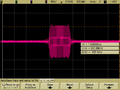
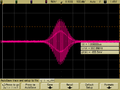
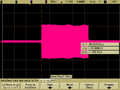
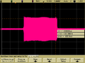
A gallery showing four of the many possible waveforms is shown below:
-
Rectangular Pulse
-
Gaussian Pulse
-
Linear Frequency Modulated Pulse
-
Nonlinear Frequency Modulated Pulse


