CSU-CHILL Receiver Front End
This article presents a new receiver front-end design for the CSU-CHILL radar.
Overview
The front-end is designed to maximize the RF dynamic range, while at the same time, preserving low noise figure and a reasonably wide RF bandwidth. The front end presents two RF channels, one per polarization.

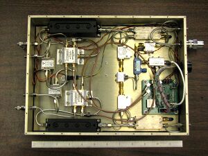
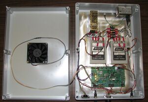
The updated front-end is comprised of a pair of low-noise Low Noise Amplifiers (LNAs), cavity filters, high speed switches, single-sideband mixers and an LO booster amplifier. A Front End monitoring system provides subsystem-level checks to verify proper operating conditions. The monitoring and power supply are housed in one sub-assembly, while the RF components are in a separate sub-assembly.
The previous front end achieved a low noise figure, thanks to the 0.7 dB noise figure LNAs. However, the LNAs have a low output compression point (+10 dBm) and a high gain (33 dB), which results in an input compression point of -23 dBm. Thus, the receiver can saturate when receiving strong echoes from nearby targets.
In addition to the LNA channels, two additional receiver channels served as the transmitter monitoring channels. These channels include the same mixers used in the main receive channels, but omit the LNAs. They are connected to Klystron outputs via a 50 dB loop coupler and a 40 dB attenuator. These channels are used to sample the Klystron output spectrum. However, transmitter output power calibration is done using a pair of average power meters.
Low Noise Amplifiers
The updated front-end features an LNA with better saturation characteristics: +13 dB output compression point, 25 dB gain, yielding an input saturation point of -12 dBm. The noise figure is 0.65 dB. Thus, the overall linear RF dynamic range of the LNA, for a 1 MHz bandwidth is -12 - (-113.9 + 0.65) = 101.25 dB.
High-speed switches
The output of the LNA is fed to a pair of high-speed switches. These switches permit the mixers to be connected to either the LNA output, or the calibration port. The calibration ports are connected to the outputs of the CHILL calibration unit, which measures the transmitted power at the radar reference plane.
The switches are driven by a pair of high-speed switch drivers, which are in turn driven by the radar timing and control subsystem. The switches are set to the calibrate position while the transmitter fires, permitting the digital receivers to make an accurate measurement of the transmitter output power, as well as the pulse shape and phase distribution. Once the transmitter has fired, the switches return to the receive position, wherein the received signal (after amplification by LNAs) is connected to the digital receiver.
The benefit of this approach is that the same, filters, mixers and digitizer are used to measure both the transmitted and received signals. The only difference is from the LNA, whose gain is separately calibrated.
Filters
Two cavity filters are used between the outputs of the high speed switches and the first mixer RF port. These filters are designed to eliminate the unwanted sideband (at 2825 MHz) from reaching the mixer, where they would be mixed down to the 50 MHz IF. This has the effect of improving the interference rejection of the radar, while also reducing the noise floor of the receiver.
The previous front-end called for the use of two tuned cavity filters of approx. 3 MHz bandwidth between the LNA and the first mixer, in order to improve the mixer noise figure by eliminating noise contribution from the unwanted mixer side band. These filters were removed, however, after they were found to adversely affect the copolar correlation coefficient (, also called ). As a result, the overall receiver noise floor was increased.
In the updated design, the filters are designed to have a 50 MHz 3dB bandwidth. Thus, gain and phase flatness of the filters over the receiver bandwidth (centered at 2725 MHz) is greatly improved over the tuned filters. Gain and phase matching between the two channels is also improved by using wider bandwidth filters. The output of the filters is padded with a 1 dB attenuator, in order to prevent gain ripple due to mismatch between the filter and the mixer outside the filter passband.
Mixers
The mixers used in the design are high-dynamic range (input P1dB of 15 dBm), image rejection mixers (also called single-sideband mixers) with an image rejection ratio of 25 dB. The mixers are tuned for lower sideband operation. The use of image rejection mixers eases the restrictions on the filter, since the mixer response from the unwanted sideband is terminated separately, rather than being allowed to mix with the IF output.
LO driver
The high-dynamic range mixers require a high LO drive signal (+17 dBm) to operate properly. The front-end includes an LO buffer amplifier, to compensate for cable losses and to provide sufficient LO drive strength. The buffer amplifier can produce +20 dBm output power, which is then split and fed through an isolator to the two mixers. The isolators are used to prevent interference between channels through the LO.
A potential failure mode for the front-end is the LO cable getting damaged, or the LO driver amplifier burning out. In order to diagnose this condition, a directional coupler is used to monitor the LO driver output. A power detector produces a DC voltage proportional to the LO driver signal strengh, which is then monitored by the Front End monitoring system.
Front-End Monitoring

The front-end monitoring system is a micro-controller based multi-purpose monitoring system. The following parameters are checked:
- Analog supply voltages
- LNA RF sub-assembly base-plate temperature
- Power Supply sub-assembly base-plate temperature
- LO drive power
- Cooling fan rotation speed
All monitored parameters are checked to see if they are within tolerance. Any out-of-tolerance parameter triggers a local alarm display. All monitored parameters and settings may be monitored and controlled through a Modbus/RTU port.
Modbus Registers
The interface to the board is through Modbus/RTU. The Modbus communications model is a single master controlling various slave devices. Each slave is addressable, and has different registers which may be read or written. This design implements read-only registers (referred to as Input Registers in the Modbus specifications) and read-write registers (Holding Registers). There are no coils or status bits available.
Input Registers
The available input registers are shown in the table below:
| Register Number | Name | Description |
|---|---|---|
| 1000 | ALARM | Indicates the cause of any alarms indicated by the Modbus ALM signal. Reading the register clears the alarm condition and deasserts the Modbus ALM signal. |
| 1001 | STATUS | Indicates the status of various subsystems in a pass/fail form |
| 1002 | 5V Voltage | The 5V analog voltage rail, in millivolts. This rail powers the power sensor and RF switches inside the Front end RF sub-assembly. |
| 1003 | 15V Voltage | The 15V analog voltage rail, in millivolts. This rail powers the LNAs and LO buffer inside the Front end RF sub-assembly. |
| 1004 | Power sensor | The power value read by the power sensor. Units TBD. |
| 1005 | Reserved | |
| 1006 | RF Sub-assembly temperature | Base-plate temperature of the RF sub-assembly. Units are 100ths of a degree, centigrade. |
| 1007 | PSU Temperature | Base-plate temperature of the power supply and monitoring sub-assembly. Units are 100ths of a degree, centigrade. |
| 1008 | Fan Speed | PSU cooling fan speed, in RPM |
Input Register Map
Alarm Register
This register contains bit values that may be used to determine the cause of an alarm/fault. The bits are described below.
| Bit | Name | Description |
|---|---|---|
| 2 | Voltage Fault | One of the monitored voltages is out of tolerance. |
| 1 | Temperature Fault | One of the monitored temperatures is out of tolerance |
| 0 | Power Fault | The LO power input to the RF sub-assembly is out of tolerance. |
ALARM register (address 1000)
Any condition that causes a fault will result in the red alarm indicator on the monitoring sub-assembly to flash. The alarm condition is cleared only by reading the ALARM register.
Status Register
This register indicates the status of various subsystems in a pass/fail form.
| Bit | Description |
|---|---|
| 3 | LO Power is within tolerance. |
| 2 | RF subsystem base-plate temperature is within tolerance |
| 1 | 15 volt analog rail is within tolerance |
| 0 | 5 volt analog rail is within tolerance |
STATUS register (address 1001)
Holding Registers
The available holding registers are shown in the table below:
| Register Number | Name | Description |
|---|---|---|
| 1000 | CONTROL | Control register |
| 1001 | MAX_TEMP | Maximum allowed base-plate temperature for RF sub-assembly |
| 1002 | MIN_5V | Lower limit for 5V analog rail |
| 1003 | MAX_5V | Upper limit for 5V analog rail |
| 1004 | MIN_15V | Lower limit for 15V analog rail |
| 1005 | MAX_15V | Upper limit for 15V analog rail |
| 1006 | PS_SCALE | Power sensor scale factor |
| 1007 | PS_OFFSET | Power sensor offset |
| 1008 | TEMP | Power sensor offset |
Holding Register Map
| Bit | Description |
|---|---|
| 0 | 0 = Power sensor output is corrected for scale/offset, 1 = Raw ADC counts for power sensor are presented. |
Control Register (address 1000)
Power Supply
The power supply for the front-end are linear types, in order to avoid any potential leakage of switching energy from switch-mode converters. EMI filters are used on the supply voltages, as well as ferrite beads and LC filters to reduce any residual noise. Since the linear supplies generate significant levels of heat, they are attached to a large aluminum base-plate, which is in turn, cooled by forced air convection. This is of particular importance in the CHILL system, since the LNAs are physically located close to the transmitters, which generate significant levels of heat.

